

In this article, we examine the effectiveness of metallic shield cans at the PCB (board) level. For this simulation study, our goal is to achieve approximately 20dB of shielding attenuation from 500MHz to 10GHz. This level of protection is often required to meet radiated immunity or emissions standards for sensitive or noisy integrated circuits (ICs).
We aim to achieve this goal using a simple shield can and a series of clips soldered onto the PCB. This setup allows for easy removal of the shield can, which is essential for rework and testing.
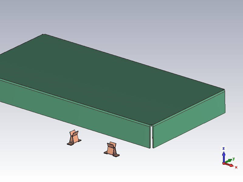
Simulation Setup
While it is generally recommended to evaluate shielding effectiveness with actual source and victim components present, we simplify the setup for this test case. We assume a plane wave impinging on the PCB and monitor the worst-case field strength at 25 locations inside the shield can across the frequency range.
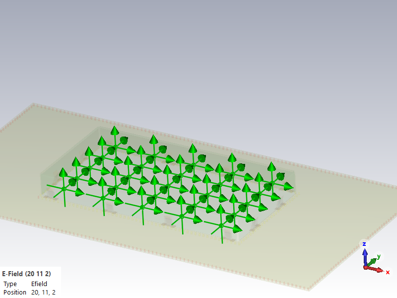
The electric field shielding effectiveness (SE) is calculated by taking the ratio of the electric field without the shield can to the electric field with the shield can. This is typically expressed in decibels (dB):
$ SE_E = 20 \log_{10} \left( \frac{E_{\text{no shield}}}{E_{\text{shield}}} \right) \quad \text{[dB]} $
Optimization 1: Number of Clips
The first optimization focuses on the number of grounding clips used.
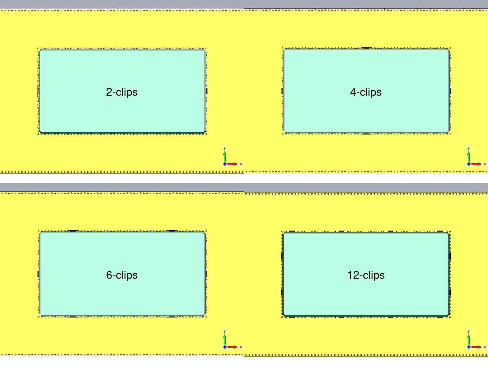
Generally, shielding effectiveness improves as the number of clips increases. However, in this test case, we observed a resonance inside the shield can that increased the internal field, resulting in negative shielding effectiveness (meaning the shield was actually amplifying the signal at specific frequencies). Adding more clips shifts this resonance to a higher frequency, moving it out of the critical band.
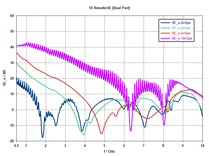
For the subsequent steps, we will use 12 clips.
Optimization 2: Internal Absorber
Another well-known method for managing resonances, especially in larger shields, is adding absorber material under the shield can. We used Laird Eccosorb® MCS with a thickness of 0.5mm. Given the shield can’s total height of 5mm, this offers a good compromise between shielding performance, weight, and space.
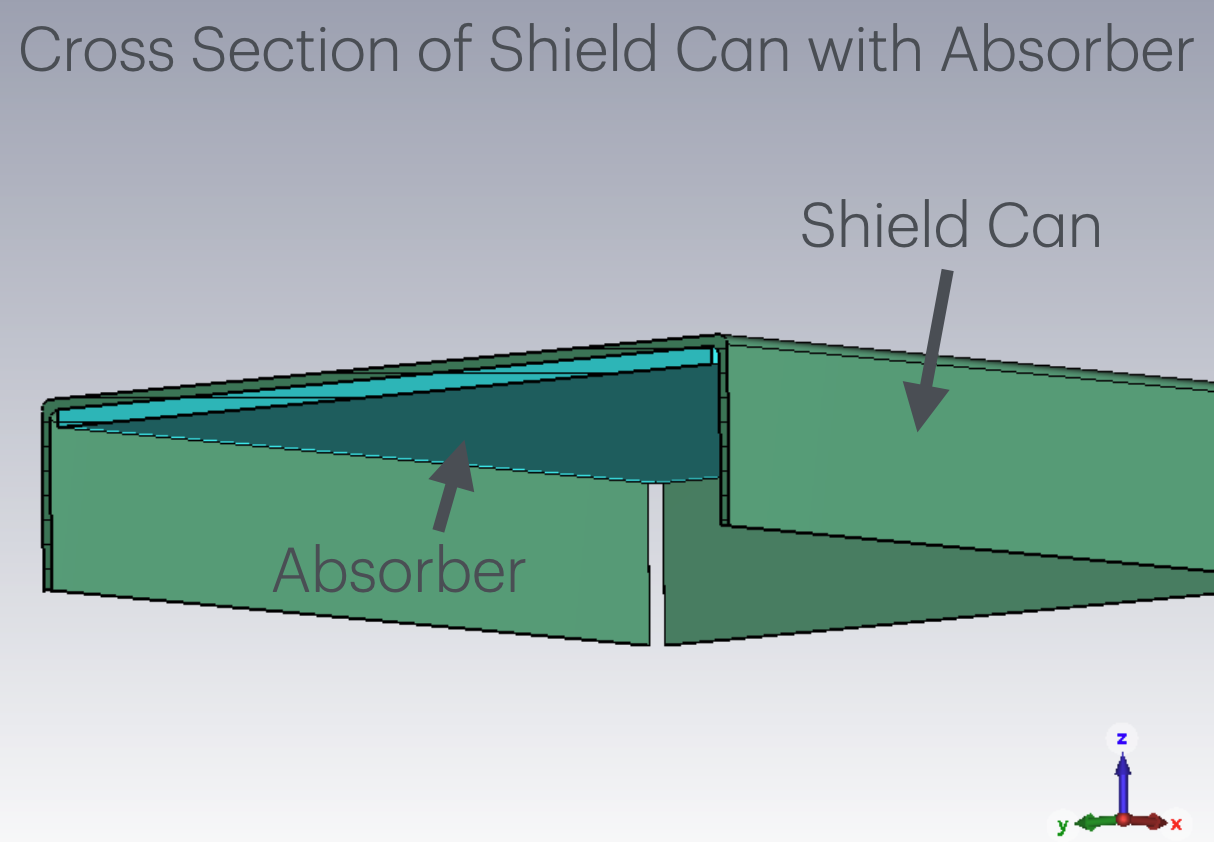
In this simulation, we expect the absorber to have little impact on the field entering the shield can, but it will dampen the field once it is inside.
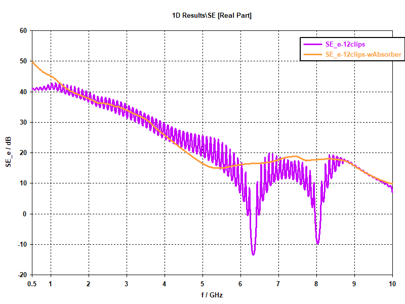
As expected, the results show that the absorber provides the most significant improvement at the resonant frequencies inside the shield can.
Optimization 3: Shield Can Cutouts
An additional design option is to lower the shield closer to the board. In the previous design, a flat-bottomed shield can would rest on top of the clips. We can lower the shield by adding cutouts around the clips.
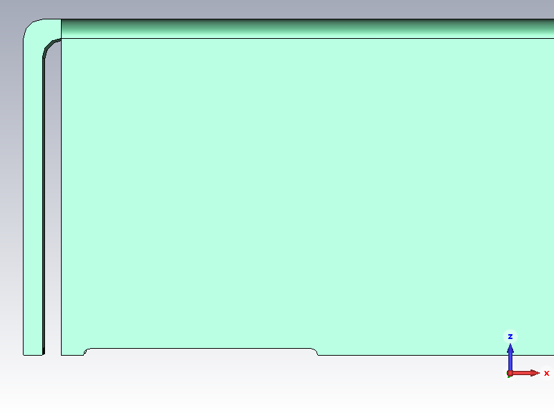
This change lowers the shield by 100µm, which increases the capacitance between the shield and the PCB ground plane around the perimeter. At high frequencies, this capacitance presents a low enough impedance to act like additional grounding connections.
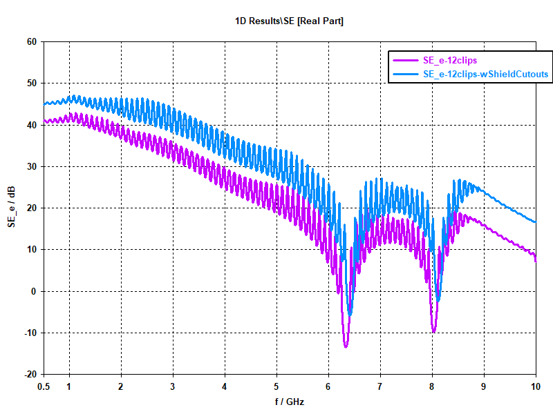
From the results, we can see that this has a significant impact on the shielding effectiveness.
Conclusion
By combining the optimized number of clips, the internal absorber, and the shield can cutouts, we achieve our design goal.
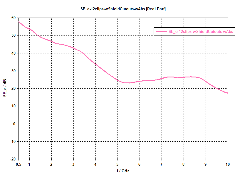
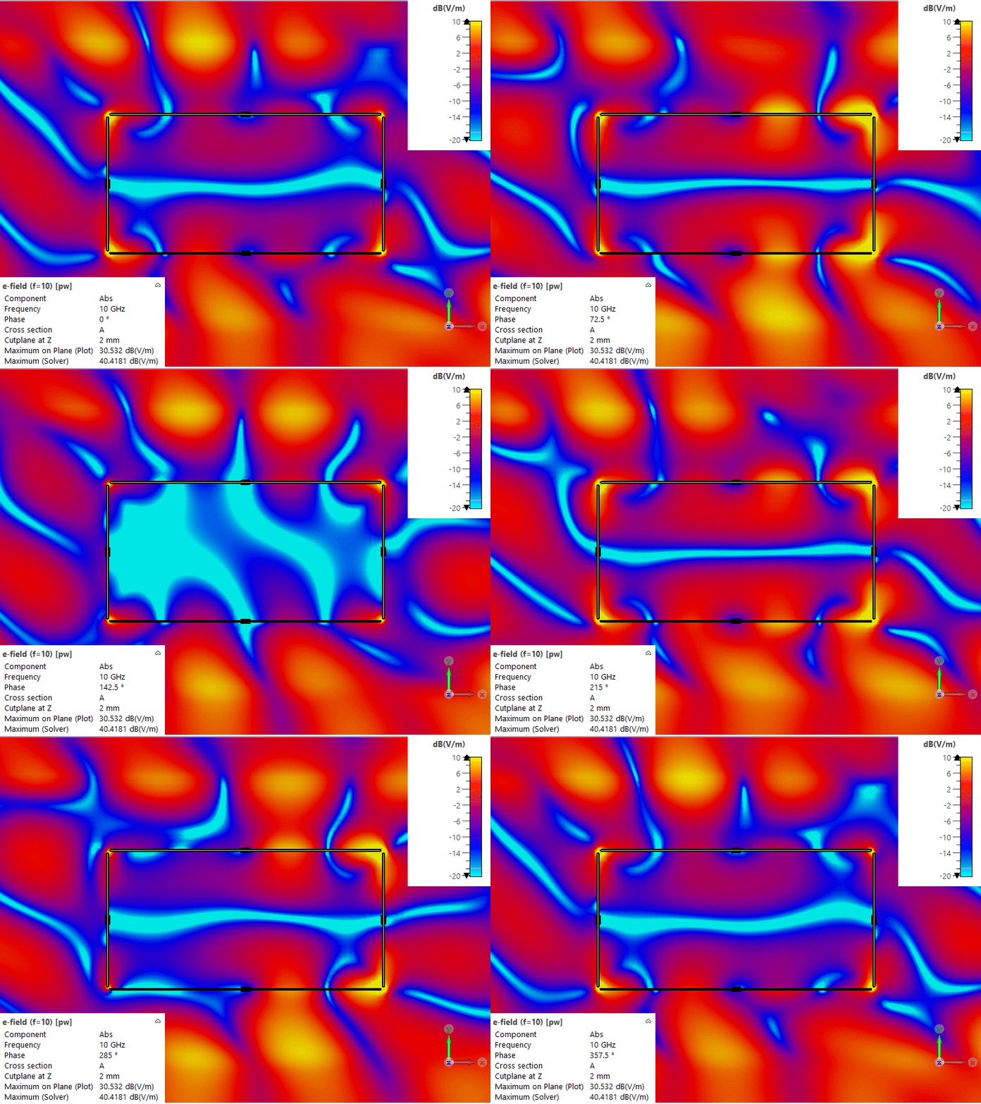
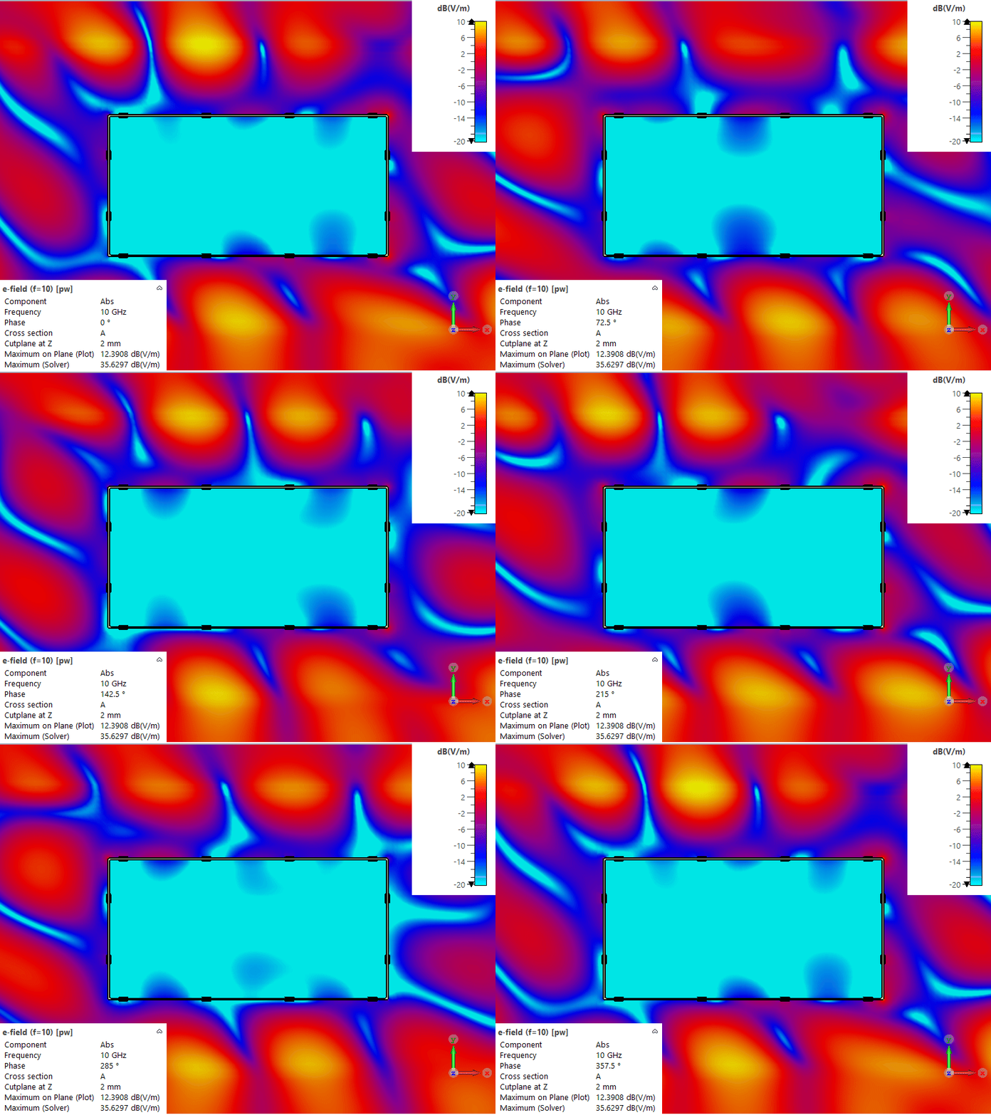
Finally, we visualize the shield in action at 10GHz. You can see how the E-field inside the shield can is significantly reduced by our design optimization compared to a 4-clip design.
4 Clip Design:
12 Clip + Absorber + Shield Can Cutouts:
Contact Us
If you have a need to optimize the shielding effectiveness of board-level shields or enclosures, feel free to reach out. We offer consulting and simulation services to help you achieve your design goals.